Introduction
The market of displays, especially low cost, high resolution, flat displays is evergrowing. In multiple applications as digital photography for example, the standard thin film transistor (TFT) displays have no longer the needed resolution. The proposed hot electron emission array makes it possible to produce displays reaching a pixel pitch of 10 μm (typical CRT displays have a pitch of 250 μm) and lessens one major drawback of other displays which is high power consumption.
A New Display Type
This feasibility study is concerned with the fabrication of an electron emitting array based on a tunnel current flowing through an array of junctions. A voltage is applied between a conducting line implanted in a silicon substrate wafer and a thin aluminium top electrode. Sandwiched between these two conductors is an insulating ultrathin SiO2 layer through which a tunnel current flows. In the tunnel process the electrons acquire a kinetic energy given by the tunnel voltage, which they may use to overcome the workfunction of the top electrode. If the aluminium top electrode is thinner than the mean free path of the electron at the given energy, the electrons travel ballistically through the electrode and are emitted in space or injected in a medium for further use. Possible uses include accelerating the electrons on astandard phosphor screen, injecting them in the promising OLED or using them for programmable e-beam lithography.
To get locally defined emission, the conductors are placed as a lattice of perpendicular lines. Electron emission takes place at the crossing points of the conductors. This configuration permits emission on each pixel independently of all others. This creates a fully addressable array of electron emitters which can be used for display applications or for projection electron lithography.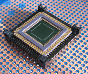
Current work focuses on developping a new process type which permits deposition of a low workfunction metal (like Al) without oxidation. Thus a process to produce the thin top electrode completely in vacuum is considered.
Fig. 1: The final hot electron emission device as mounted on a chip carrier. The experimental setup permits measurements of an array of up to 32×32 pixels