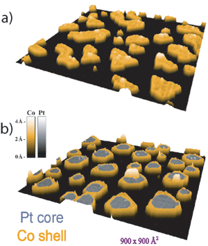
Edge atoms do all the work. 3D view of an STM image of (a) one monolayer high Co and (b) one monolayer high islands with a Pt core and an approximately 3 atom wide Co shell (deposition of 0.2 ML Pt at 130 K and annealing to 760 K generates the quasi hexagonal non-magnetic core; subsequent deposition of 0.2 ML Co at 220 K creates the Co rim). In the STM images, Co can be discerned from Pt by its 0.3 Å larger apparent height which was used as color code. The temperature dependence of the zero field susceptibility reveals that the Co-rim χ Pt-core islands have the same anisotropy as the pure Co islands with equal perimeter length.
Testing facilities
A UHV chamber (base pressure 3 x 10-11 mbar) was used for the preparation and in-situ characterization of the metallic nanostructures. This system provides full control of sample temperature (20 – 800 K) for growth, morphology characterization with Scanning Tunneling Microscopy (STM), and the acquisition of magnetic hysteresis loops with Surface Magneto Optical Kerr Effect (SMOKE).
Project results:
2D magnetism: The original magnetic properties of nanometer sized particles are due to the distinct contributions of volume, surface, and step atoms. To disentangle these contributions is an ongoing challenge of material science. Here we introduce a method enabling to identify the indeed strikingly different contributions of surface and perimeter atoms to the magnetic anisotropy energy of 2D nanostructures. Our method uses the generally non-linear relationship between perimeter length and surface area. Atomic-scale characterization of the morphology of ensembles of polydisperse nanostructures combined with in-situ measurements of their temperature dependent magnetic susceptibility gives access to the role played by the differently coordinated atoms. We show for Co nanostructures on a Pt(111) surface that their uniaxial out-of-plane magnetization is entirely caused by edge atoms having 20 times more anisotropy energy than their bulk and surface counterparts. Identification of the role of perimeter and surface atoms opens up unprecedented opportunities for material engineering. As an example we separately tune magnetic hardness and moment in bi-metallic core-shell nanostructures. [S. Rusponi et al. Nature Materials 2, 546 (2003)]
Periodic arrays of 2D nanostructures: We produced highly ordered arrays of two atomic layer high Co dots by using self-organized growth on a vicinal Au(788) surface. This surface has equidistant steps and reconstructed (111) terraces with domain walls running perpendicular to the step edges. Since nucleation of Co dots can be confined to the intersections of reconstruction domain walls and steps, this surface provides a template for the creation of lattices with a pitch size of 3.5 nm x 7.0 nm which are phase coherent over the entire sample surface, of the order of 1 cm2. We found that: (i) the Co particles are characterized by an extremely narrow MAE distribution with half width at half maximum of about 17%, a factor two better than the best result achieved in arrays of monodisperse colloidal particles [S. I. Woods et al., Phys. Rev. Lett. 87, 137205 (2001)], (ii) all particles have uniaxial out-of-plane anisotropy, surmounting the drawback of colloidal particles with randomly oriented easy magnetization axis reducing the signal-to-noise ratio in future industrial applications, and (iii) the temperature dependence of χ demonstrates the absence of inter-particle interactions up to a density of 26 Tdots/in²[N. Weiss et al. Phys. Rev. Lett. 95, 157204 (2005)].
Outlook
We intend:
- to exploit the effect of reduced coordination in novel structures containing mainly step atoms and yielding units containing only 2000 atoms with stable magnetization at 300 K.
- to extend our investigations to Co/Pt/Ru, Fe/Pt, and Fe/Pd element combinations in order to increase the MAE/atom and thereby to stabilize even smaller particles in their out-of-plane magnetization up to 300 K.
- to individually read the islands in arrays with densities of up to 10 T dots/in2 by means of spin-polarized STM [M. Bode et al., Phys. Rev. Lett. 86, 2142 (2001), W. Wulfhekel and J. Kirschner, Appl. Phys. Lett. 75, 1944 (1999)].
- to attempt to write individual bits by injection of a spin-polarized current from the STM-tip. This writing technique is based on current induced magnetization reversal recently found in transport of a spin-polarized current through magnetic nanostructures [E. B. Myers et al., Science 285, 867 (1999); J. E. Wegrowe et al., Europhys. Lett. 45, 626 (1999); W. Weber, Science 291, 1015 (2001)].